
File:Two layer board.jpg: Difference between revisions
No edit summary |
(No difference)
|
Latest revision as of 20:30, 19 September 2023
Side view of the edge of a circuit board, showing that the inside layers of the board are all fiberglass with no conducting metal.
File history
Click on a date/time to view the file as it appeared at that time.
| Date/Time | Thumbnail | Dimensions | User | Comment | |
|---|---|---|---|---|---|
| current | 20:30, 19 September 2023 | 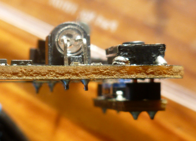 | 400 × 288 (92 KB) | Adamw (talk | contribs) |
You cannot overwrite this file.
File usage
The following page uses this file: